The Semiconductor Revolution: Transistors, Photolithography & TSMC
Encyclopedia/2. Technology & The Built World/1. Computing, AI & Information Technology/01. Hardware & Electronics • Curated by Admin Timeline.sg
The semiconductor revolution traces the evolution from the first transistor at Bell Labs in 1947 to today's advanced 2nm chip nodes, highlighting key innovations like the integrated circuit, photolithography, and the TSMC foundry model that enabled the digital age.
Chronological Storyline (44 Milestones)
Dec 23, 1947 CE
Invention of the Point-Contact Transistor
John Bardeen, Walter Brattain, and William Shockley at Bell Labs demonstrate the first working point-contact transistor, a germanium-based device that amplifies electrical signals. This invention replaces bulky vacuum tubes and lays the foundation for modern electronics. #transistor #electronics
Invention of the Point-Contact Transistor By Federal employee - https://clintonwhitehouse4.archives.gov/Initiatives/Millennium/capsule/mayo.html, Public domain, https://commons.wikimedia.org/w/index.php?curid=554340
Jul 1, 1948 CE
Shockley Develops the Junction Transistor
William Shockley invents the junction transistor, a more practical and reliable design than the point-contact transistor. This device uses semiconductor layers and becomes the basis for mass-produced transistors. #transistor #semiconductor
Shockley Develops the Junction Transistor By Mister rf at English Wikipedia - Own work, CC BY-SA 3.0, https://commons.wikimedia.org/w/index.php?curid=11885148
1952 CE
Bell Labs Licenses Transistor Technology
Bell Labs licenses its transistor technology to other companies for a fee, sparking widespread commercial development. This includes licenses to Texas Instruments, Sony, and others, accelerating the adoption of transistors in consumer electronics. #transistor #business
Bell Labs Licenses Transistor Technology By Ulfbastel - Own work, CC BY-SA 3.0, https://commons.wikimedia.org/w/index.php?curid=3123331
Oct 18, 1954 CE
First Silicon Transistor by Texas Instruments
Gordon Teal of Texas Instruments demonstrates the first commercial silicon transistor, which offers better performance and higher temperature tolerance than germanium. Silicon becomes the dominant semiconductor material. #silicon #transistor
1956 CE
Nobel Prize for Transistor Invention
John Bardeen, Walter Brattain, and William Shockley are awarded the Nobel Prize in Physics for their research on semiconductors and the discovery of the transistor effect. This recognition cements the transistor's importance. #Nobel #transistor
Sep 12, 1958 CE
Jack Kilby Invents the Integrated Circuit
Jack Kilby at Texas Instruments demonstrates the first working integrated circuit, a phase-shift oscillator built on a single piece of germanium. This invention integrates multiple components on one chip, revolutionizing electronics. #integratedcircuit #invention
Jack Kilby Invents the Integrated Circuit By cole8888, https://flickr.com/photos/187597251@N05/ (aka Cole L) - https://www.flickr.com/photos/187597251@N05/49899342293/, CC BY-SA 2.0, https://commons.wikimedia.org/w/index.php?curid=95653492
Jan 23, 1959 CE
Robert Noyce Files Patent for Planar Integrated Circuit
Robert Noyce at Fairchild Semiconductor files a patent for a planar integrated circuit using silicon and aluminum interconnects. This design becomes the standard for IC manufacturing, enabling mass production. #integratedcircuit #patent
Robert Noyce Files Patent for Planar Integrated Circuit By Robert.Baruch - Own work, CC BY-SA 4.0, https://commons.wikimedia.org/w/index.php?curid=57750460
1961 CE
First Commercial Integrated Circuit by Fairchild
Fairchild Semiconductor releases the first commercial integrated circuit, the Micrologic flip-flop. This marks the beginning of the IC market, initially used in military and aerospace applications. #integratedcircuit #commercial
First Commercial Integrated Circuit by Fairchild By Fairchild Semiconductor - http://www.fairchildsemi.com/, Public domain, https://commons.wikimedia.org/w/index.php?curid=26763160
1963 CE
CMOS Logic Invented by Frank Wanlass
Frank Wanlass at Fairchild Semiconductor patents CMOS (complementary metal-oxide-semiconductor) logic, which consumes very little power. CMOS becomes the dominant technology for digital integrated circuits. #CMOS #logic
CMOS Logic Invented by Frank Wanlass By Abaddon1337 - Own work, CC BY-SA 3.0, https://commons.wikimedia.org/w/index.php?curid=19163930
Apr 19, 1965 CE
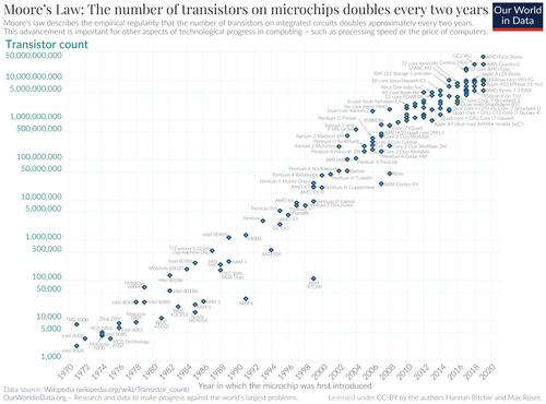
Moore's Law Published
Gordon Moore, co-founder of Fairchild and later Intel, publishes a paper predicting that the number of transistors on a chip will double every year. This prediction, later revised to every two years, becomes a driving force for the semiconductor industry. #MooresLaw #prediction
Moore's Law Published By Max Roser, Hannah Ritchie - https://ourworldindata.org/uploads/2020/11/Transistor-Count-over-time.png, CC BY 4.0, https://commons.wikimedia.org/w/index.php?curid=98219918
1967 CE
First MOS Memory Chip by Fairchild
Fairchild Semiconductor introduces the first MOS (metal-oxide-semiconductor) memory chip, a 64-bit SRAM. This demonstrates the potential of MOS technology for high-density memory, leading to DRAM and flash memory. #memory #MOS
Jul 18, 1968 CE
Intel Corporation Founded
Robert Noyce and Gordon Moore leave Fairchild to found Intel, which becomes the world's largest semiconductor company. Intel focuses on memory chips and later microprocessors, driving the PC revolution. #Intel #founding
Intel Corporation Founded By Coolcaesar - Own work, CC BY-SA 4.0, https://commons.wikimedia.org/w/index.php?curid=133964425
1970 CE
First DRAM Chip by Intel
Intel introduces the 1103, the first commercially available dynamic random-access memory (DRAM) chip. This 1-kilobit chip replaces magnetic core memory and becomes a standard for computer memory. #DRAM #memory
First DRAM Chip by Intel By Thomas Nguyen - Own work, CC BY-SA 4.0, https://commons.wikimedia.org/w/index.php?curid=49532861
Nov 15, 1971 CE
Intel 4004 Microprocessor Released
Intel releases the 4004, the first commercial microprocessor, integrating a 4-bit CPU on a single chip. This invention enables programmable electronics and sparks the microprocessor revolution. #microprocessor #Intel
Intel 4004 Microprocessor Released By Thomas Nguyen - Own work, CC BY-SA 4.0, https://commons.wikimedia.org/w/index.php?curid=47684767
1974 CE
Intel 8080 Microprocessor
Intel introduces the 8080, an 8-bit microprocessor that becomes the CPU for early personal computers like the Altair 8800. Its success establishes Intel as a leader in microprocessors. #microprocessor #Intel
Intel 8080 Microprocessor By The Science Museum UK - [1], CC BY 4.0, https://commons.wikimedia.org/w/index.php?curid=133514392
Jun 8, 1978 CE
Intel 8086 Microprocessor Launched
Intel launches the 8086, a 16-bit microprocessor that introduces the x86 architecture. This architecture becomes the foundation for most PC processors, including modern Intel and AMD chips. #x86 #microprocessor
Intel 8086 Microprocessor Launched By Thomas Nguyen - Own work, CC BY-SA 4.0, https://commons.wikimedia.org/w/index.php?curid=46809082
Oct 17, 1985 CE
Intel 80386 Microprocessor
Intel releases the 80386 (386), a 32-bit microprocessor with on-chip memory management. This chip enables multitasking operating systems like Windows and Linux, driving the PC era. #microprocessor #Intel
Intel 80386 Microprocessor By Konstantin Lanzet (with permission) - CPU collection Konstantin Lanzet, received per EMailCamera: Canon EOS 400D, CC BY-SA 3.0, https://commons.wikimedia.org/w/index.php?curid=4213308
1986 CE
ASML Founded
ASML (Advanced Semiconductor Materials Lithography) is founded in the Netherlands as a joint venture between Philips and ASM International. ASML becomes the world's leading supplier of photolithography systems for chip manufacturing. #ASML #lithography
ASML Founded By A ansems - Own work, Public domain, https://commons.wikimedia.org/w/index.php?curid=4092531
Feb 21, 1987 CE
TSMC Founded
Taiwan Semiconductor Manufacturing Company (TSMC) is founded by Morris Chang as the world's first dedicated semiconductor foundry. TSMC's pure-play foundry model revolutionizes the industry by allowing fabless chip design companies to manufacture without owning fabs. #TSMC #foundry
TSMC Founded By 曾 成訓 - https://www.flickr.com/photos/tsengphotos/53114942112/, CC BY 2.0, https://commons.wikimedia.org/w/index.php?curid=147718717
1989 CE
First Commercial ASML Stepper (PAS 2500)
ASML ships its first commercial stepper, the PAS 2500, which uses a step-and-repeat method for photolithography. This system improves resolution and throughput, enabling smaller transistor geometries. #ASML #stepper
1991 CE
First 0.5 Micron Process by TSMC
TSMC achieves 0.5-micron process technology, marking a milestone in semiconductor manufacturing. This allows for higher transistor density and better performance, attracting major customers like AMD and NVIDIA. #TSMC #process
1993 CE
Intel Pentium Processor Released
Intel launches the Pentium processor, a superscalar x86 CPU with a 60 MHz clock speed. The Pentium brand becomes synonymous with high-performance computing and drives the multimedia PC boom. #Pentium #Intel
Intel Pentium Processor Released By Intel Corporation - https://www.intel.com/content/www/us/en/products/details/processors/pentium.html, Public domain, https://commons.wikimedia.org/w/index.php?curid=132640549
1995 CE
TSMC 0.35 Micron Process
TSMC introduces its 0.35-micron process, enabling higher integration and lower power consumption. This process is used for graphics chips, logic ICs, and other advanced applications. #TSMC #process
1997 CE
Copper Interconnects Introduced by IBM
IBM announces the use of copper interconnects instead of aluminum in semiconductor chips. Copper reduces resistance and improves performance, becoming the standard for advanced nodes. #copper #interconnect
1999 CE
TSMC 0.18 Micron Process
TSMC ramps its 0.18-micron process, which becomes a workhorse for many fabless companies. This node enables high-performance graphics and networking chips, fueling the dot-com era. #TSMC #process
2000 CE
First 300mm Wafer Fab by TSMC
TSMC opens its first 300mm wafer fabrication facility, Fab 12, in Hsinchu, Taiwan. Larger wafers reduce cost per chip and increase productivity, setting a new industry standard. #TSMC #wafer
2002 CE
Intel Introduces 90nm Process with Strained Silicon
Intel launches its 90nm process technology featuring strained silicon, which increases transistor speed. This innovation helps Intel maintain its lead in process technology. #Intel #process
2004 CE
TSMC 65nm Process
TSMC begins production of 65nm chips, offering significant power and performance improvements. This node is used for mobile processors and graphics chips, supporting the rise of smartphones. #TSMC #process
2006 CE
First High-k/Metal Gate Transistors by Intel
Intel introduces high-k dielectric and metal gate materials in its 45nm process, reducing leakage current and improving performance. This innovation extends Moore's Law and is adopted industry-wide. #highk #transistor
2008 CE
TSMC 40nm Process
TSMC launches its 40nm process, a half-node shrink from 45nm. This node is used for graphics processors and mobile SoCs, enabling higher performance in consumer electronics. #TSMC #process
2010 CE
First 28nm Process by TSMC
TSMC introduces its 28nm process, which becomes one of the most successful nodes in history. It offers a balance of performance, power, and cost, used in countless mobile and networking chips. #TSMC #process
2011 CE
Intel 22nm Tri-Gate (FinFET) Transistors
Intel introduces the first commercial FinFET (tri-gate) transistors in its 22nm process. This 3D structure improves control over current and reduces leakage, enabling continued scaling. #FinFET #transistor
Intel 22nm Tri-Gate (FinFET) Transistors By Д.Ильин: vectorization - File:Doublegate FinFET.PNG by Irene Ringworm at English Wikipedia, Public domain, https://commons.wikimedia.org/w/index.php?curid=132333446
2012 CE
ASML Ships First EUV Lithography Prototype
ASML delivers the first extreme ultraviolet (EUV) lithography prototype, the NXE:3100, to research labs. EUV uses 13.5nm wavelength light to enable finer patterning for advanced nodes. #EUV #lithography
ASML Ships First EUV Lithography Prototype By 2pem - Own work, CC BY-SA 3.0, https://commons.wikimedia.org/w/index.php?curid=30619878
2014 CE
TSMC 16nm FinFET Process
TSMC begins production of its 16nm FinFET process, adopting 3D transistor technology. This node powers many high-end mobile processors and GPUs, including Apple's A9 chip. #TSMC #FinFET
2015 CE
First EUV Production Tool by ASML
ASML ships its first production-ready EUV lithography system, the NXE:3300, to customers. EUV begins to be used for critical layers in advanced nodes, reducing the need for multiple patterning. #EUV #ASML
2017 CE
TSMC 7nm Process Enters Production
TSMC starts volume production of its 7nm process, offering 40% higher performance or 60% lower power compared to 10nm. This node is used for Apple's A12 Bionic and AMD's Ryzen processors. #TSMC #7nm
2018 CE
EUV Lithography Adopted for 7nm+ by TSMC
TSMC uses EUV lithography for some layers in its 7nm+ process, marking the first high-volume use of EUV. This reduces process complexity and improves yield. #EUV #TSMC
2019 CE
TSMC 5nm Process Announced
TSMC announces its 5nm process, which uses EUV for more layers and offers 15% speed improvement or 30% power reduction over 7nm. This node is used for Apple's A14 and M1 chips. #TSMC #5nm
2020 CE
TSMC 5nm Volume Production
TSMC begins volume production of 5nm chips, becoming the first foundry to do so. This node powers flagship smartphones and high-performance computing, solidifying TSMC's technological leadership. #TSMC #5nm
2021 CE
Intel Announces IDM 2.0 Strategy
Intel announces a new strategy to become a major foundry player, investing billions in new fabs and opening its manufacturing to external customers. This shifts the competitive landscape. #Intel #foundry
2022 CE
TSMC 3nm Process Enters Production
TSMC starts production of its 3nm process (N3), offering up to 15% speed gain and 30% power reduction over 5nm. This node is used for Apple's A17 Pro and M3 chips. #TSMC #3nm
2023 CE
ASML Ships First High-NA EUV System
ASML delivers the first high-NA (numerical aperture) EUV lithography system, the Twinscan EXE:5000, to Intel. High-NA EUV enables even smaller features for sub-3nm nodes. #EUV #ASML
2024 CE
TSMC 2nm Process Development
TSMC announces its 2nm process (N2) using nanosheet transistors (GAAFET), promising significant performance and efficiency gains. Production is expected in 2025. #TSMC #2nm
2025 CE
Intel 18A Process Expected
Intel plans to launch its 18A (1.8nm) process with RibbonFET (GAA) and PowerVia (backside power delivery). This node aims to regain process leadership. #Intel #process