Encyclopedia/2. Technology & The Built World/1. Computing, AI & Information Technology • Curated by Admin Timeline.sg
This timeline traces the evolution of semiconductor lithography from its early origins to the modern era, highlighting key innovations, pivotal figures, and the rise of TSMC as a global foundry leader. It covers the foundational inventions, process node breakthroughs, and the development of advanced lithography technologies like EUV.
Chronological Storyline (40 Milestones)
Dec 23, 1947 CE
Invention of the Transistor
John Bardeen, Walter Brattain, and William Shockley at Bell Labs demonstrate the first point-contact transistor, laying the foundation for modern electronics. #transistor #electronics
Invention of the Transistor By Ulfbastel - Own work, CC BY-SA 3.0, https://commons.wikimedia.org/w/index.php?curid=3123331
1951 CE
Shockley Develops Junction Transistor
William Shockley invents the junction transistor, which is more practical for mass production. #transistor #semiconductor
Shockley Develops Junction Transistor By Mister rf at English Wikipedia - Own work, CC BY-SA 3.0, https://commons.wikimedia.org/w/index.php?curid=11885148
1955 CE
Early Photolithography for Transistors
Researchers at Bell Labs and other institutions develop photolithography techniques to pattern transistor features on semiconductor wafers. #lithography #semiconductor
Early Photolithography for Transistors By Rob Bulmahn - https://www.flickr.com/photos/rbulmahn/49913961083/, CC BY 2.0, https://commons.wikimedia.org/w/index.php?curid=152547842
Sep 12, 1958 CE
Jack Kilby Invents the Integrated Circuit
Jack Kilby at Texas Instruments demonstrates the first integrated circuit, merging multiple transistors on a single germanium chip. #IC #integratedcircuit
Jack Kilby Invents the Integrated Circuit By cole8888, https://flickr.com/photos/187597251@N05/ (aka Cole L) - https://www.flickr.com/photos/187597251@N05/49899342293/, CC BY-SA 2.0, https://commons.wikimedia.org/w/index.php?curid=95653492
Jan 23, 1959 CE
Robert Noyce Patents Planar Integrated Circuit
Robert Noyce at Fairchild Semiconductor patents a planar IC using silicon, enabling mass production. #IC #silicon
Robert Noyce Patents Planar Integrated Circuit By Robert.Baruch - Own work, CC BY-SA 4.0, https://commons.wikimedia.org/w/index.php?curid=57750460
1961 CE
First Commercial Integrated Circuit
Fairchild Semiconductor releases the first commercial IC, the F101, using photolithography. #IC #lithography
First Commercial Integrated Circuit By Fairchild Semiconductor - http://www.fairchildsemi.com/, Public domain, https://commons.wikimedia.org/w/index.php?curid=26763160
1963 CE
CMOS Invented
Frank Wanlass at Fairchild invents complementary metal-oxide-semiconductor (CMOS) logic, which later dominates low-power chip design. #CMOS #logic
CMOS Invented By Abaddon1337 - Own work, CC BY-SA 3.0, https://commons.wikimedia.org/w/index.php?curid=19163930
Apr 19, 1965 CE
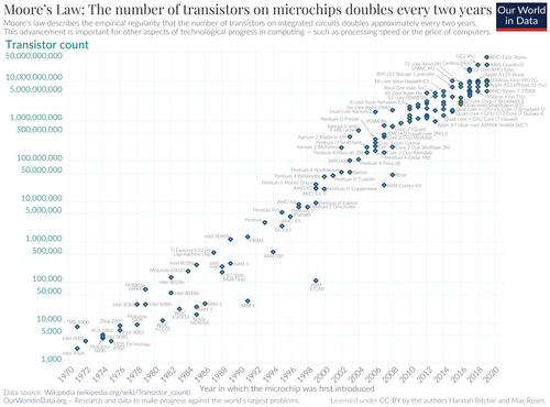
Moore's Law Published
Gordon Moore observes that transistor density doubles every two years, predicting the pace of semiconductor advancement. #MooresLaw #semiconductor
Moore's Law Published By Max Roser, Hannah Ritchie - https://ourworldindata.org/uploads/2020/11/Transistor-Count-over-time.png, CC BY 4.0, https://commons.wikimedia.org/w/index.php?curid=98219918
Jul 18, 1968 CE
Intel Founded
Robert Noyce and Gordon Moore found Intel, which becomes a leader in memory and microprocessor chips. #Intel #semiconductor
Intel Founded By Coolcaesar - Own work, CC BY-SA 4.0, https://commons.wikimedia.org/w/index.php?curid=133964425
Nov 15, 1971 CE
Intel 4004 Microprocessor
Intel releases the 4004, the first commercial microprocessor, with 2,300 transistors using 10 µm lithography. #microprocessor #Intel
Intel 4004 Microprocessor By Thomas Nguyen - Own work, CC BY-SA 4.0, https://commons.wikimedia.org/w/index.php?curid=47684767
1973 CE
First Projection Lithography System
Perkin-Elmer introduces the Micralign projection mask aligner, improving resolution over contact printing. #lithography #projection
1978 CE
Step-and-Repeat Lithography Introduced
GCA Corporation develops the first commercial wafer stepper (DSW 4800), enabling finer patterns. #lithography #stepper )
1980 CE
64K DRAM Achieved
Hitachi and others produce 64K DRAM chips using advanced lithography, pushing design rules below 2 µm. #DRAM #memory
64K DRAM Achieved By ZeptoBars - http://zeptobars.ru/en/read/how-to-open-microchip-asic-what-inside, CC BY 3.0, https://commons.wikimedia.org/w/index.php?curid=25043835
1984 CE
ASML Founded
ASML (Advanced Semiconductor Materials Lithography) is established in the Netherlands, later becoming the dominant lithography equipment supplier. #ASML #lithography
ASML Founded By A ansems - Own work, Public domain, https://commons.wikimedia.org/w/index.php?curid=4092531
1986 CE
TSMC Construction Begins
The Taiwanese government initiates the construction of TSMC's first fab in Hsinchu Science Park. #TSMC #foundry
TSMC Construction Begins By 曾 成訓 - https://www.flickr.com/photos/tsengphotos/53114942112/, CC BY 2.0, https://commons.wikimedia.org/w/index.php?curid=147718717
Feb 21, 1987 CE
TSMC Founded by Morris Chang
Morris Chang establishes Taiwan Semiconductor Manufacturing Company, the world's first dedicated semiconductor foundry. #TSMC #MorrisChang
TSMC Founded by Morris Chang By 總統府 - 11.21 2020 APEC暨經濟領袖會議會後記者會, CC BY 2.0, https://commons.wikimedia.org/w/index.php?curid=170534279
1988 CE
TSMC's First Fab Operational
TSMC's Fab 2 begins production, offering CMOS processes for logic chips. #TSMC #fab
1990 CE
i-line Lithography Adopted
Nikon and Canon ship i-line (365 nm) steppers, enabling mass production of 0.5 µm devices. #lithography #i-line
Mar 22, 1993 CE
Intel Pentium Processor
Intel launches the Pentium with 0.8 µm lithography, containing 3.1 million transistors. #Intel #Pentium
Intel Pentium Processor By Intel Corporation - https://www.intel.com/content/www/us/en/products/details/processors/pentium.html, Public domain, https://commons.wikimedia.org/w/index.php?curid=132640549
1995 CE
TSMC Listed on NYSE
TSMC becomes publicly traded on the New York Stock Exchange, raising capital for expansion. #TSMC #IPO
1997 CE
Copper Interconnects Introduced
IBM unveils copper wiring instead of aluminum, reducing resistance and allowing faster chips. #copper #interconnect
1999 CE
0.18 µm Node Reached
TSMC and others achieve 0.18 µm lithography, enabling copper interconnects and higher performance. #lithography #node
2001 CE
EUV Lithography Research Gains Momentum
ASML, Intel, and others invest in extreme ultraviolet (EUV) lithography for future nodes. #EUV #lithography
EUV Lithography Research Gains Momentum By 2pem - Own work, CC BY-SA 3.0, https://commons.wikimedia.org/w/index.php?curid=30619878
2003 CE
90 nm Node with Strained Silicon
Intel introduces strained silicon at the 90 nm node, enhancing transistor performance. #strainedsilicon #90nm
2004 CE
TSMC Becomes World's Largest Foundry
TSMC surpasses competitors in revenue and capacity, solidifying its leadership. #TSMC #foundry
2005 CE
65 nm Node in Production
TSMC and Intel begin volume production at 65 nm with improved power efficiency. #65nm #lithography
2007 CE
45 nm Node with High-k/Metal Gate
Intel introduces high-k dielectric and metal gate at 45 nm, reducing leakage. #highk #45nm
ASML delivers the NXE:3100, a prototype EUV lithography system, for early development. #EUV #ASML
2011 CE
TSMC's 28 nm Node Becomes Major Success
TSMC ramps 28 nm process, widely adopted by major chip designers for its performance and power balance. #28nm #TSMC
2012 CE
20 nm Node Development
TSMC begins development of the 20 nm process, using planar transistors. #20nm #lithography
2014 CE
TSMC Introduces 16 nm FinFET
TSMC's 16 nm FinFET process delivers significant power and performance gains over planar transistors. #FinFET #16nm
TSMC Introduces 16 nm FinFET By Д.Ильин: vectorization - File:Doublegate FinFET.PNG by Irene Ringworm at English Wikipedia, Public domain, https://commons.wikimedia.org/w/index.php?curid=132333446
2016 CE
TSMC Ramps 10 nm Production
TSMC begins volume production of the 10 nm node, used in Apple A10X and Huawei Kirin 970. #10nm #TSMC
2017 CE
ASML Delivers First EUV Production Tools
ASML ships the NXE:3300, a production-ready EUV scanner, to leading chipmakers. #EUV #ASML
2018 CE
TSMC Begins 7 nm Volume Production
TSMC's 7 nm node enables chips like Apple A12 and AMD Zen 2, with EUV used in later versions. #7nm #TSMC
2020 CE
5 nm Node Enters Production
TSMC starts mass production of the 5 nm node (N5), used in Apple A14 and M1 chips. #5nm #TSMC
Jun 1, 2021 CE
TSMC Announces Arizona Fab
TSMC announces plans to build a 5 nm fab in Arizona, USA, to diversify global chip supply. #TSMC #Arizona
Dec 29, 2022 CE
TSMC Begins 3 nm Volume Production
TSMC starts commercial production of the 3 nm node (N3), used in Apple A17 and M3 chips. #3nm #TSMC
2023 CE
TSMC Announces 2 nm Node
TSMC reveals its 2 nm (N2) process with nanosheet transistors, targeting production in 2025. #2nm #TSMC
2024 CE
High-NA EUV Lithography Delivered
ASML ships the first high-NA EUV (0.55 NA) system to Intel, enabling sub-2 nm patterning. #HighNA #EUV