Sumerian metalworkers in Mesopotamia systematically alloyed copper with tin to produce bronze, creating stronger tools and weapons and establishing metallurgy as a foundational craft. · Wikipedia: https://en.wikipedia.org/wiki/Bronze_Age
Map of the diffusion of metallurgy. By User:Want - File:Diffusion métallurgie.png: After M. Otte (2007) Vers la Préhistoire, de Boeck, Bruxelles, CC BY-SA 3.0 cz, https://commons.wikimedia.org/w/index.php?curid=41316620
2500 BCE
Andean gold and silver metallurgy emerges
Indigenous Andean peoples in modern-day Peru developed sophisticated gold and silver metallurgy by around 2500 BCE, creating intricate alloys and decorative objects well before European contact. Source — Wikipedia:
Ceremonial knife (tumi) from Sicán in Peru. 850-1050 AD; Ethnological Museum, Berlin, Germany By User:FA2010 - Own work, Public domain, https://commons.wikimedia.org/w/index.php?curid=15350592
500 BCE
Chinese cast iron blast furnaces
By the 5th century BCE, Chinese metallurgists operating blast furnaces produced cast iron on a large scale, enabling advanced agricultural tools and weapons centuries before Europe achieved similar capability. Source — Wikipedia:
Mat weight in the shape of a tiger Tomb 1 Dayun Mountain Xuyi Jiangsu Western Han 2nd century BCE Bronze inlaid with gold and silver (cleaned up) By Mary Harrsch - This image has been extracted from another file, CC BY-SA 4.0, https://commons.wikimedia.org/w/index.php?curid=145764124
300 BCE
Wootz crucible steel produced in India
Indian metalworkers in the Deccan region began producing wootz, a high-carbon crucible steel renowned for its sharpness and distinctive patterns, later traded to the Middle East where it became the basis for Damascus steel blades. Source — Wikipedia:
Watered pattern on iranian sword blade. By Rahil Alipour Ata Abadi - Transferred from en.wikipedia to Commons., GFDL, https://commons.wikimedia.org/w/index.php?curid=50800188
200 BCE
Porcelain developed in China
Chinese potters in the Han dynasty or earlier developed proto-porcelain, evolving by the Tang dynasty into true porcelain — a material whose controlled kaolin clay and high-temperature firing process was unmatched globally for over a millennium. Source — Wikipedia:
Porcelain developed in China By 国立文化財機構 - ColBase: Integrated Collections Database of the National Museums, Japan: online database: entry tnm/TG-3051, CC BY 4.0, https://commons.wikimedia.org/w/index.php?curid=120319431
100 CE
West African bronze casting at Igbo-Ukwu
Artisans in what is now southeastern Nigeria created sophisticated bronze and copper castings using the lost-wax technique at Igbo-Ukwu, demonstrating advanced indigenous metallurgy with distinctive local styles. Source — Wikipedia:
9th century bronze staff head in form of a coiled snake found in Igbo-Ukwu, Anambra State, Nigeria. Located in the National Museum Onikan, Lagos, Nigeria. By Ochiwar - Own work, CC BY-SA 3.0, https://commons.wikimedia.org/w/index.php?curid=29327025
800 CE
Jabir ibn Hayyan systematizes metallurgy
The Persian-Arab alchemist Jabir ibn Hayyan wrote extensively on the purification of metals such as gold, silver, and iron, introducing systematic laboratory techniques that influenced medieval metallurgy and materials processing. Source — Wikipedia:
15th-century artistic impression of Jabir ibn Hayyan (Geber) from Codici Ashburnhamiani 1166, Biblioteca Medicea Laurenziana, Florence fol 12r By Unknown author - https://cdn.britannica.com/10/132710-050-CECF006B/illustration-manuscript-Abu-Musa-Jabir-ibn-Hayyan.jpg, Public domain, https://commons.wikimedia.org/w/index.php?curid=166835469
1100 CE
Zinc distillation at Zawar, India
Indian metallurgists at Zawar in Rajasthan developed the distillation of zinc from ore by the 12th century, the earliest known production of metallic zinc in the world, enabling brass manufacture on a new scale. Source — Wikipedia:
1590 CE
Microscope reveals material microstructure
Zacharias and Hans Janssen (and later Antoni van Leeuwenhoek) developed optical microscopes that allowed humans to observe material microstructure for the first time, laying the groundwork for understanding material properties at small scales. Source — Wikipedia:
A vintage optical microscope in a Ukrainian classroom. By Ann 2000 - Микроскоп.JPG, CC BY-SA 4.0, https://commons.wikimedia.org/w/index.php?curid=138936770
Aug 24, 1856 CE
Bessemer process enables mass steel
Henry Bessemer patented a process for mass-producing steel cheaply by blowing air through molten pig iron to remove impurities, revolutionizing construction and manufacturing worldwide. Source — Wikipedia:
Bessemer process enables mass steel By Unknown author, Public domain, https://commons.wikimedia.org/w/index.php?curid=91836The Bessemer Process Explained in 3 Minutes — How Steel Built the Modern World
1863 CE
Sorby pioneers metallography
Henry Clifton Sorby developed metallographic microscopy techniques to examine the microstructure of steel and iron, establishing the field of metallography and demonstrating that material properties depend on internal structure. Source — Wikipedia:
Sorby pioneers metallography By Chemical Engineer - Own work, Public domain, https://commons.wikimedia.org/w/index.php?curid=7687614
Apr 8, 1911 CE
Kamerlingh Onnes discovers superconductivity
Heike Kamerlingh Onnes discovered superconductivity — zero electrical resistance — in mercury cooled to 4.2 K with liquid helium, launching an entirely new field of physics and materials research. · Wikipedia: https://en.wikipedia.org/wiki/Superconductivity
A high-temperature (liquid nitrogen cooled) superconductor levitating above a permanent magnet (TU Dresden) By Henry Mühlpfordt - Own work, CC BY-SA 3.0, https://commons.wikimedia.org/w/index.php?curid=9491383How Superconductivity Was Discovered
1931 CE
Ruska invents the electron microscope
Ernst Ruska and Max Knoll built the first transmission electron microscope, achieving magnifications far beyond optical microscopes and enabling direct imaging of material structures at the nanometer scale. · Wikipedia: https://en.wikipedia.org/wiki/Electron_microscope
The ASTEM is an FEI Titan³ G2 60-300. By Alice im Miniland - Own work, CC BY-SA 4.0, https://commons.wikimedia.org/w/index.php?curid=42485910
1953 CE
Watson and Crick determine DNA structure
James Watson and Francis Crick, using Rosalind Franklin's X-ray diffraction data, determined the double-helix structure of DNA, a landmark in understanding biological materials at the molecular level. · Wikipedia: https://en.wikipedia.org/wiki/Nucleic_acid_double_helix
Static thumb frame of Animation of the structure of a section of DNA. The bases lie horizontally between the two spiraling strands. By 84user adapting file originally uploaded by Richard Wheeler (Zephyris) at en.wikipedia - Derived from File:DNA orbit animated.gif originally from here., CC BY-SA 3.0, https://commons.wikimedia.org/w/index.php?curid=6285050The DNA Double Helix Discovery — HHMI BioInteractive Video
Dec 29, 1959 CE
Feynman envisions nanotechnology
Richard Feynman gave a lecture titled 'There's Plenty of Room at the Bottom,' envisioning the manipulation of matter at the atomic scale and laying the conceptual foundation for nanotechnology. Source — Wikipedia:
There's Plenty of Room at the Bottom - Richard Feynman
1962 CE
Josephson effect predicted
Brian Josephson predicted that supercurrents could tunnel through a thin insulating barrier between two superconductors, a phenomenon now central to superconducting electronics and quantum metrology. · Wikipedia: https://en.wikipedia.org/wiki/Josephson_effect
One-volt en:voltage standard developed by en:NIST (formerly en:National Bureau of Standards (NBS) until 1988) based on an array of 3020 superconducting en:Josephson junctions, operating at liquid-helium temperatures. Microwave energy fed into the finguide structure on the left generates a voltage across the 4 chains of junctions on the right. By NBS - NIST paper A Practical Josephson Voltage Standard at One Volt, Figure 1, Public domain, https://commons.wikimedia.org/w/index.php?curid=319467
1974 CE
Taniguchi coins 'nanotechnology'
Norio Taniguchi of Tokyo University of Science coined the term 'nanotechnology' to describe precision materials processing at the nanometer scale, giving the emerging field its modern name. Source — Wikipedia:
1981 CE
STM images individual atoms
Gerd Binnig and Heinrich Rohrer at IBM Zurich invented the scanning tunneling microscope, capable of imaging individual atoms on material surfaces and revolutionizing nanoscale materials characterization. Source — Wikipedia:
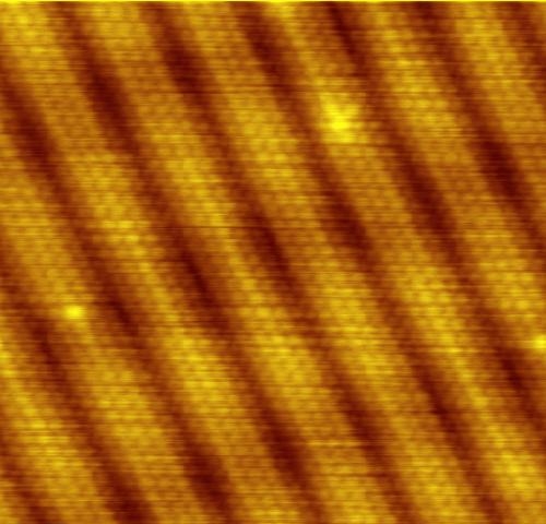
Image of surface reconstruction on a clean Gold (Au(100)) surface, as visualized using scanning tunneling microscopy. The individual atoms composing the material are visible. Surface reconstruction causes the surface atoms to deviate from the bulk crystal structure, and arrange in columns several atoms wide with regularly spaced pits between them. Technical details: Atomically resolved STM image of clean Au(100). This image is made with hjjnh GBhh an Omicron Low Temperature STM and RHK Technology electronics by Erwin Rossen, Eindhoven University of Technology, 2006. Parameters: p<1e-11 mbar, T is 77 K, I_setpoint is 6 nA, V_bias is 1 mV, Au(100) surface is Ar sputtered (1,5 kV, 2uA, 30 minutes) and annealed (500°C, 30 minutes). By Erwinrossen - en:File:Atomic_resolution_Au100.JPG, see upload log, Public domain, https://commons.wikimedia.org/w/index.php?curid=1790142
1985 CE
Buckminsterfullerene discovered
Harry Kroto, Richard Smalley, and Robert Curl discovered buckminsterfullerene (C60), a spherical carbon molecule of 60 atoms, opening the field of carbon nanomaterials and earning the 1996 Nobel Prize in Chemistry. · Wikipedia: https://en.wikipedia.org/wiki/Buckminsterfullerene
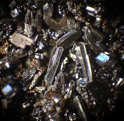
C60 Buckminsterfullerene, crystallized. From the Leopold-Franzens-Universität Innsbruck. By Fotograf: Jochen Gschnaller - German Wikipedia, original upload Dez 2004 by Moebius1 (selfmade), CC BY-SA 3.0, https://commons.wikimedia.org/w/index.php?curid=350278
1986 CE
High-temperature cuprate superconductors
J. Georg Bednorz and K. Alex Müller discovered superconductivity in copper oxide ceramics at 35 K, far above previous limits, launching the era of high-temperature superconductors and winning the 1987 Nobel Prize in Physics. Source — Wikipedia:
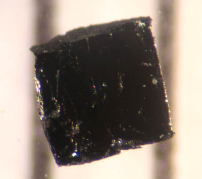
A small sample of the high-temperature superconductor, Bi-2223. By James Slezak, Cornell Laboratory of Atomic and Solid State Physics - Own work, CC BY 2.5, https://commons.wikimedia.org/w/index.php?curid=864046
1991 CE
Iijima discovers carbon nanotubes
Sumio Iijima of NEC Corporation reported the discovery of carbon nanotubes, cylindrical carbon nanostructures with extraordinary mechanical and electrical properties that became central to nanotechnology research. · Wikipedia: https://en.wikipedia.org/wiki/Carbon_nanotube
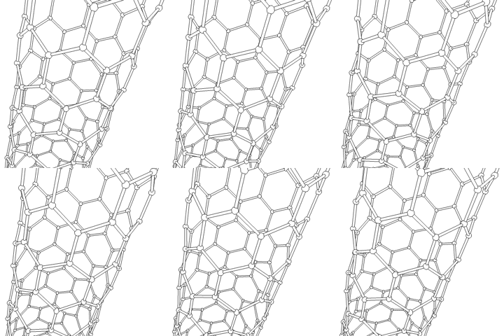
Carbon nanotube By Original hochgeladen von Schwarzm am 30. Aug 2004; Selbst gemacht mit C4D/Cartoonrenderer, GNU FDL - German Wikipedia, original upload 29. Dez 2004 by APPER, CC BY-SA 3.0, https://commons.wikimedia.org/w/index.php?curid=350208
1996 CE
First optical metamaterial demonstrated
Researchers constructed a composite material with a negative refractive index at microwave frequencies, demonstrating the first practical metamaterial with electromagnetic properties not found in nature. Source — Wikipedia:
Figure 2 Part of the left-handed metamaterial array configuration, which was constructed of copper split-ring resonators and wires mounted on interlocking sheets of fiberglass circuit board. The total array consists of 3 by 20 by 20 unit cells with overall dimensions of 10 by 100 by 100 mm. Split-ring resonator consisting of an inner square with a split on one side embedded in an outer square with a split on the other side. Split-ring resonators are on the front and right surfaces of the square grid, and single vertical wires are on the back and left surfaces. References: Chevalier, Christine T.; and Wilson, Jeffrey D.: Frequency Bandwidth Optimization of Left-Handed Metamaterial. NASA/TM--2004-213403, 2004. Wilson, Jeffrey D.; and Schwartz, Zachary D.: Multifocal Flat Lens With Left-Handed Metamaterial. Appl. Phys. Lett., vol. 86, no. 2, 2005. Smith, D.R., et al.: Composite Medium With Simultaneously Negative Permeability and Permittivity. Phys. Rev. Lett., vol. 84, no. 18, 2000. Shelby, R.A., et al.: Microwave Transmission Through a Two-Dimensional, Isotropic, Left-Handed Metamaterial. Appl. Phys. Lett., vol. 78, no. 4, 2001. By Jeffrey.D.Wilson@nasa.gov (Glenn research contact) - NASA Glenn Research, Public domain, https://commons.wikimedia.org/w/index.php?curid=7455771
2004 CE
Graphene isolated by Geim and Novoselov
Andre Geim and Konstantin Novoselov isolated graphene — a single layer of carbon atoms — using mechanical exfoliation with Scotch tape, revealing extraordinary strength and conductivity and winning the 2010 Nobel Prize in Physics. · Wikipedia: https://en.wikipedia.org/wiki/Graphene
The ideal crystalline structure of graphene is a hexagonal grid. By AlexanderAlUS - Own work, CC BY-SA 3.0, https://commons.wikimedia.org/w/index.php?curid=11294534Professor Konstantin Novoselov interviewed about Graphene
2006 CE
Invisibility cloak using metamaterials
David Smith's group at Duke University demonstrated a metamaterial 'invisibility cloak' that redirected microwave radiation around an object, validating transformation optics as a practical materials design paradigm. Source — Wikipedia:
Diagram of a solenoid and its magnetic field lines. The shape of all lines was computed according to the laws of electrodynamics. By Geek3 - Own work, CC BY-SA 3.0, https://commons.wikimedia.org/w/index.php?curid=10618762
2008 CE
Iron-based superconductors discovered
Hideo Hosono and colleagues discovered superconductivity in iron-based pnictide compounds at 26 K, establishing a new family of high-temperature superconductors and expanding the search beyond copper oxides. Source — Wikipedia:
Structure of LnFePnOF superconductors, Ln = lanthanide (La, Ce, etc.), Pn = pnictide (As, P, etc.) By Materialscientist - Own work, CC BY-SA 3.0, https://commons.wikimedia.org/w/index.php?curid=40347835
2014 CE
Perovskite solar cells surpass 20% efficiency
Researchers achieved over 20% power conversion efficiency with perovskite-structured solar cells, a new class of solution-processable photovoltaic materials that rapidly transformed the energy materials landscape. Source — Wikipedia:
"The U.S. Department of Energy Solar Energy Technologies Office (SETO) supports research and development projects that increase the efficiency and lifetime of hybrid organic-inorganic perovskite solar cells, speeding the commercialization of perovskite solar technologies and decreasing manufacturing costs." "What are Perovskite Solar Cells? Halide perovskites are a family of materials that have shown potential for high performance and low production costs in solar cells. The name “perovskite” comes from the nickname for their crystal structure, although other types of non-halide perovskites (such as oxides and nitrides) are utilized in other energy technologies, such as fuel cells and catalysts. Perovskite solar cells have shown remarkable progress in recent years with rapid increases in efficiency, from reports of about 3% in 2009 to over 25% today. While perovskite solar cells have become highly efficient in a very short time, a number of challenges remain before they can become a competitive commercial technology." By Dennis Schroeder / National Renewable Energy Laboratory - https://www.energy.gov/eere/solar/perovskite-solar-cells, Public domain, https://commons.wikimedia.org/w/index.php?curid=131749994
2018 CE
Magic-angle twisted bilayer graphene
Pablo Jarillo-Herrero's group at MIT discovered that twisting two graphene layers by a 'magic angle' of about 1.1 degrees produces superconductivity, launching the field of twistronics and moiré materials. · Wikipedia: https://en.wikipedia.org/wiki/Twistronics
Moiré pattern arising from the superposition of two graphene lattices twisted by 4°. By Ponor - Own work, CC BY-SA 4.0, https://commons.wikimedia.org/w/index.php?curid=91250759
A Korean team (Lee et al.) claimed room-temperature superconductivity in a lead-apatite compound called LK-99, sparking global replication efforts; the claims were not independently verified and were attributed to impurities. · Wikipedia: https://en.wikipedia.org/wiki/LK-99
Pellet of LK-99 being repelled by a magnet By Hyun-Tak Kim - https://sciencecast.org/casts/suc384jly50n, CC BY 4.0, https://commons.wikimedia.org/w/index.php?curid=135452379